加速 IC 設計和新封裝引進 NPI
在當今競爭激烈的半導體領域,快速將創新的 IC 設計和先進的封裝推向市場對於保持市場領先地位至關重要。隨著設計複雜性的增加和上市時間的縮短,工程團隊需要整合的解決方案來簡化從概念到製造的工作流程。您可以加速創新,同時確保品質。

優化半導體開發流程
全面的半導體設計和製造解決方案可確保從概念到生產所有階段的無縫整合。透過採用整體方法,半導體公司可以加速積體電路設計、改進 3D 積體電路封裝並實現卓越製造。
A comprehensive approach to IC design innovation combines integrated project management, cross-domain collaboration and digital twin technology to accelerate semiconductor development and unlock new business opportunities. Our solution helps you:
- Drive faster development cycles through real-time collaboration across product teams, quality, process engineering and manufacturing in a semiconductor-specific environment.
- Leverage digital twin technology to optimize designs from chip-level through advanced IC, enabling seamless integration from specification to fabrication.
- Embed sustainability early in product design to significantly reduce environmental impact while meeting performance goals.
- Streamline NPI success with automated project management templates, out-of-the-box metrics, and unified program delivery platforms.
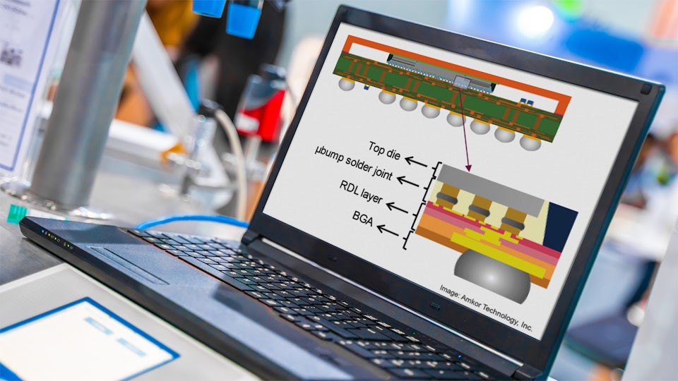
Empower your business with a comprehensive approach to 3D IC design that tackles the increasing complexities of heterogeneous packaging while unlocking greater functionality. Here's how our integrated solution advances your success:
- Streamline ASIC and chipset integration through an accessible, scalable solution that reduces dependency on specialized expertise.
- Ensure digital continuity through unified data models that enable efficient design and predictive analysis.
- Implement strategies that capitalize on 3D IC form factor advantages while managing manufacturing complexity.
- Adopting a modular approach enhances performance and significantly reduces development costs and time-to-market for semiconductor products.
Adopting a comprehensive approach to semiconductor manufacturing that combines early planning integration, yield optimization, and end-to-end traceability. You can minimize manufacturing issues and accelerate production readiness, ensuring high yields in today's complex manufacturing environment. The key benefits of our manufacturing-focused solution include:
- Address manufacturing challenges early in the design phase through streamlined DFT, compression, and ATPG optimization that aligns with foundry requirements.
- Ensure production readiness by connecting all digital and physical assets in one efficient data and process model, from die design through bill of process.
- Strengthen security and quality control through comprehensive traceability that prevents disruptions, counterfeits, and potential security breaches.
統一 IC 設計與先進封裝的優勢
2030 年的產業成長
利用統一設計和先進的封裝解決方案來利用前所未有的半導體市場成長,特別是在汽車、運算和無線領域。
設備引腳管理
透過統一的解決方案對高度複雜的半導體封裝進行全面的設計驗證,簡化整合過程,同時保持品質和性能。
縮短上市時間
透過統一設計和先進封裝推動創新,滿足快速成長的需求。
Smarter, faster, greener AI with 3D IC chiplet advanced packaging
ETRI and Amkor
Electronics, Semiconductor devices
USA, South Korea
Calibre, Xpedition IC Packaging
西門子 IC 封裝設計工具幫助我們為客戶提供快速、高品質的設計服務,即使是大型封裝和晶片封裝結構。
探索我們的資源庫
透過我們全面的資源庫加速 IC 設計創新。取得實用指南、技術深度探討和真實案例研究,以了解應對當今半導體挑戰的有效方法。透過根據您的需求量身定制的專家見解來提高效率、優化製造準備並簡化開發週期。
